Intel’s EMIB-T Yield Just Surged. Can It Break the AI Packaging Bottleneck?
Reported EMIB substrate yield rose from 20–25% to about 45%, lifting good output by 80%. Stable customer volume is the next test.
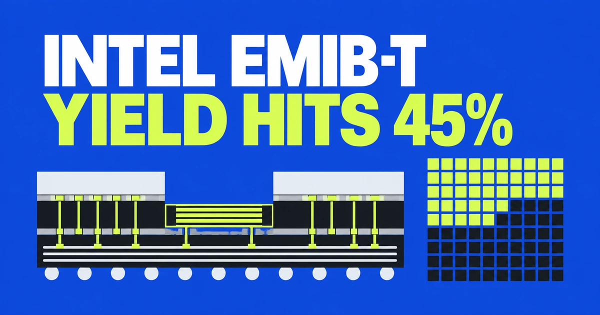
- A Jefferies analysis cited by Keypost puts Intel’s EMIB substrate yield at about 45%, up from 20–25% in the second quarter, with 50% targeted by the end of September.
- EMIB-T embeds small silicon bridges only where chips need dense links, then adds through-silicon vias for vertical power delivery.
- Higher yield can unlock far more usable substrates without adding equipment, but Intel still has to turn that gain into repeatable delivery for customer AI products.
The reported yield is not the yield of Intel’s compute dies. It is the yield of the advanced package substrate that embeds Intel’s EMIB bridges. That figure has reportedly climbed from 20–25% in the second quarter to roughly 45%, turning 100 substrate starts from 25 usable units into 45.
A move from 25% to 45% means 80% more good substrates
Yield percentages are easy to underestimate. At 25% yield, a batch of 100 substrates produces 25 usable units. At 45%, the same input produces 45. The absolute gain is 20 substrates, but the usable output is 80% higher.
| Substrates started | Yield | Good substrates | Gain versus 25% |
|---|---|---|---|
| 100 | 25% | 25 | Baseline |
| 100 | 45% | 45 | 80% |
| 100 | 50% | 50 | 100% |
The figures come from an industry analysis reported by Keypost rather than a confirmed Intel production disclosure. Their importance lies in what they imply about a manufacturing problem that has limited usable EMIB packaging.
Compute dies can leave the wafer fab while accelerators still miss shipment
An AI accelerator combines large compute dies with stacks of high-bandwidth memory. Those parts must sit close together and communicate through extremely dense wiring. Advanced packaging supplies that connection.
TSMC’s CoWoS became a critical production step for this reason. A foundry can produce the compute dies successfully, yet the accelerator cannot ship until those dies and HBM are integrated into one working package. Packaging capacity controls real AI hardware supply alongside wafer capacity.
Size makes the problem harder. A large rectangular interposer yields fewer complete pieces from a round wafer, while more material is lost at the edge. Increasing wafer throughput does not translate one-for-one into finished packages when each package consumes a larger area.
EMIB-T uses silicon only where the connection needs it
CoWoS-S places a broad silicon interposer beneath the compute dies and HBM. Fine wiring runs through that interposer, which then sits on a separate package substrate.
Intel’s EMIB takes a local approach. Small silicon bridges sit beneath the boundaries where two dies need dense connections. The bridges are embedded directly into the organic package substrate, avoiding a full sheet of interposer silicon.
EMIB-T adds through-silicon vias to the bridge. Those vertical paths supplement die-to-die signaling with power delivery from below. As compute dies and HBM stacks grow, power loss and voltage stability become more difficult to control.
| Approach | Dense connection location | Defining structure |
|---|---|---|
| CoWoS-S | Broad silicon interposer | Silicon spans the compute and memory area |
| CoWoS-L | Local silicon links inside an RDL interposer | RDL supports a larger package with localized silicon |
| Intel EMIB-T | Silicon bridges embedded in the organic substrate | Local bridges add TSV-based vertical power delivery |
Removing the large interposer moves precision work into the substrate
The economic appeal is straightforward. Small bridge dies can be produced in quantity, then embedded while multiple substrates are formed on a large panel. Compute dies and HBM are attached afterward. Intel avoids manufacturing a large silicon interposer for every package.
The substrate process becomes harder in exchange. Each bridge must be aligned laterally and vertically. A chip mounted above it connects to contacts on both the bridge and the surrounding substrate. If one surface sits too high or too low, some joints may fail to connect.
Silicon and organic substrate materials also expand at different rates as temperature changes. Warping during assembly or operation can stress the joints. EMIB reduces the burden of a large interposer, but its substrate suppliers inherit demanding bridge placement, fine-line routing and material-control work.
Better yield changes both supply and cost
When substrate yield rises, the same equipment can send more good units into package assembly. Less material and process time are discarded for every acceptable substrate. That matters because poor substrate yield can consume the cost advantage EMIB was designed to create.
The point at which a defect is found also changes the loss. Catch it during substrate inspection and the loss ends with the substrate. Find it after attaching expensive compute dies and HBM, and those components may be lost with it.
No single company controls the whole result. Substrate vendors must embed the bridges and connect the fine routing. Intel supplies the interconnect technology and design rules, attaches the chips and validates the completed package. Customer volume appears only when those steps reach the same quality and production schedule.
Intel’s opening is a US-based path to a finished AI package
Intel already operates advanced packaging infrastructure in New Mexico. If EMIB-T production stabilizes for outside customers, a chip produced in the United States could also be packaged there instead of crossing the Pacific for advanced integration.
Geography alone will not win an order. A customer needs a compatible contact layout and power-delivery design, completed performance and reliability qualification, and dependable substrate supply. Technical compatibility and manufacturing timing have to converge before a design becomes a shipped product.
TSMC and Amkor are also expanding US advanced-packaging capacity. Intel’s opportunity is time-sensitive: secure customer designs and stabilize volume production before competing domestic options reach scale.
Forty-five percent is manufacturing progress, not a finished victory
A rise from 25% to 45% would show meaningful progress in one of EMIB-T substrate manufacturing’s central bottlenecks. It would deliver 80% more usable substrates from the same number of starts, reduce wasted processing per good unit and improve the odds of catching defects before expensive dies and HBM are attached.
Customers do not buy a yield chart. They buy a guaranteed quantity of working packages delivered on schedule. Intel still has to reproduce the improved yield across its substrate partners and convert it into predictable output.
The next evidence will be a customer AI chip using EMIB-T that reaches launch on time and ships at the promised volume. The reported yield surge says the substrate process is moving. Whether Intel becomes a true CoWoS alternative will be decided when that number turns into finished hardware.
Frequently asked questions
What is Intel EMIB-T?
EMIB-T embeds small silicon bridges in the package substrate to connect compute dies and HBM. It adds through-silicon vias to provide a vertical power-delivery path through the bridge.
Why does moving from 25% to 45% yield mean 80% more good output?
A batch of 100 substrates produces 25 good units at 25% yield and 45 at 45%. The additional 20 units are an 80% increase over the original 25. It does not mean equipment capacity grew by 80%.
Can 45% yield make Intel an immediate replacement for TSMC CoWoS?
No. Intel and its substrate partners still need repeatable quality, customer qualification and dependable volume on the customer product schedule.
How does EMIB-T differ from CoWoS-S?
CoWoS-S uses a broad silicon interposer below compute and memory dies. EMIB-T places small silicon bridges only at dense connection boundaries and embeds them directly in the organic substrate.